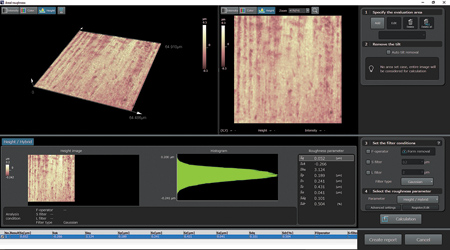
Areal roughness data for a lead frame die pad (data provided by Olympus LEXT OLS5000).
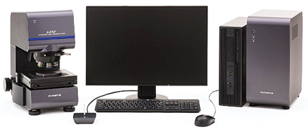
The Olympus LEXT OLS5000 3-D measuring laser microscope set, including microscope frame, monitor and control boxes.
Circuit technology continues to develop rapidly, fueled by increasing worldwide demand for electronic products. Semiconductors are essential components of circuits, making their manufacture a high-tech, detail-oriented business. The manufacturing process consists of wafer fabrication, integrated circuit (IC) design, photo masking, IC packaging, IC assembly, testing, and lead frame, connector and board manufacture. During each step, defects introduced during the manufacturing process can lead to product failures. Consequently, technologies for semiconductor inspection that are sensitive, fast and cost-effective are badly needed.
The small size and complexity of semiconductor chips make inspecting them a challenge. In this article, we review the inspection difficulties and discuss how modern laser scanning confocal microscopes meet or exceed the industry's inspection requirements. We also demonstrate the advantages of laser scanning confocal microscopes for one of the most challenging parts of semiconductor inspection-measuring the surface roughness of a lead frame die pad.
IC Packaging Inspection Challenges
The wafer IC manufacturing process is complex. Circuit patterns are etched onto a silicon wafer after a coating of a photosensitive layer is deposited. Because of the extremely small size of the circuit structure, any contaminants or flaws can cause defects in the surface of the wafer IC, so the surface profile of the reticle and wafer IC must be tested. In addition, as the demand for denser circuits increases, so does the complexity of the IC packages. Fusion of these technologies requires an inspection tool with high accuracy, speed and the ability to precisely measure small 3-D structures composed of different materials.
Another important measurement is surface roughness. Surface metrology provides value in discovering functional correlations between roughness and performance/processing. Understanding the 3-D surface texture is essential for defining irregular features. In the semiconductor industry, the quality of silicon wafers is directly related to the quality of fabricated wafer IC chips. The preparation of silicon wafers requires dozens of processes to give them a smooth, mirror-like polished surface. After the wafer is etched, the back surface of the prepared wafer IC needs to be thinned, according to the application requirements. To thin it, the back side of the wafer IC is subjected to rough grinding followed by fine grinding. The roughness of the surface must be monitored during this process. In addition, a lead frame is used to support the chip mechanically during the assembly of plastic packages and to connect the chip electrically with the outside world. During semiconductor manufacturing, a diced IC chip is picked up and mounted on the lead frame's die pad. The surface roughness is critical for proper adherence on the pad.
How Laser Confocal Microscopes Solve the Challenges of Semiconductor Inspection
Performing surface metrology on wafers or chips requires microscopes with nanoscale resolution. Laser confocal microscopes offer fast, noncontact and nondestructive 3-D observations and measurements with high vertical and lateral resolution. High-quality laser confocal microscopes offer easy-to-use software so that, with a few button presses, users can measure fine shapes at the submicron level.
With the capability to make accurate 3-D measurements on a wide range of sample types, laser scanning microscopes deliver reliable data for semiconductor quality assurance and process control. Some new systems even offer automatic data acquisition, so complicated setting adjustments may be unnecessary. This enables users with minimal training to obtain accurate results from their microscopy system.
Inspecting the Roughness of Lead Frame Die Pad
During semiconductor manufacturing, a diced IC chip is mounted on the die pad of a lead frame. Before the chip is mounted, an adhesive paste is applied to the die pad, and the pad's roughness directly impacts the paste's adhesiveness. Typically, manufacturers would measure this surface roughness using a contact stylus or a white-light interferometer, but there are problems with both tools.
A contact stylus with a diamond tip can easily damage sensitive structures, such as a die pad. In addition, the roughness data it can acquire is limited by the size of the stylus' tip, and most are 2 µm at the smallest, making them unsuitable for micron-sized roughness measurements. With the tip contaminated with surface materials, the measurements cannot be consistent or accurate. White-light interferometers maintain a sub-nanoscale resolution for smooth surfaces, but the congestion of interference patterns prevents accurate measurement for steeply inclined surfaces (rough surfaces or features with slopes). The numerical aperture of the interference objective lens on white-light interferometers is normally smaller than that used on optical microscopes with lower horizontal resolution. Atomic force microscopes (AFM) are capable of sub-nanometer resolution measurement with a much smaller tip (1-10 nm) than contact stylus profilers. However, they are slow (minutes per image) and are confined to imaging a very small area (<100 µm). AFM tips are expensive consumables, and the system requires highly experienced users.
The use of a laser scanning microscope overcomes these limitations. In this example, we used an Olympus LEXT OLS5000 laser microscope to demonstrate its effectiveness at measuring a die pad's surface roughness. Laser scanning confocal microscopes make measurements without touching the sample. For sensitive samples, like die pads, this is advantageous since there is less chance of causing damage and contamination during the inspection. The laser also provides superior resolution over a stylus. The microscope's high-quality optics provide fast and accurate roughness measurement in multiscale analysis. It can achieve a vertical resolution down to 6 nm and a lateral resolution down to 120 nm. With built-in ISO standards on both line and areal roughness acquisition and analysis, users can determine the most suitable measurement conditions and parameters for their application. It only takes seconds to acquire a sample image and process the data.
The microscope's stitching function is also useful in this application. Instead of capturing a single field of view for roughness measurements, the microscope can measure roughness across an entire plane with fast stitching. While roughness is acquired as numerical data, the microscope also displays it as three types of image data-a color image, a laser image and a height image.
Conclusion
Inspecting the tiny microstructures of a semiconductor is a challenging inspection application. Older methods, such as a contact stylus, white-light interferometer and atomic force microscope, can damage the sample or do not provide the resolution required by today's manufacturers. Using a laser scanning confocal microscope, on the other hand, offers numerous advantages. These microscope systems can quickly and accurately inspect and characterize the geometry of wafers, chips and other components. Three dimensional surface images, advanced functionality and easy-to-use software enable users with minimal training to acquire the accurate, precise data semiconductor manufacturers require.
Authored by Mina Hong, Olympus Applications Scientist, Industrial Metrology
For more information contact:
Olympus Scientific Solutions Americas
48 Woerd Ave.
Waltham, MA 02453
800-225-8330
www.olympus-ims.com